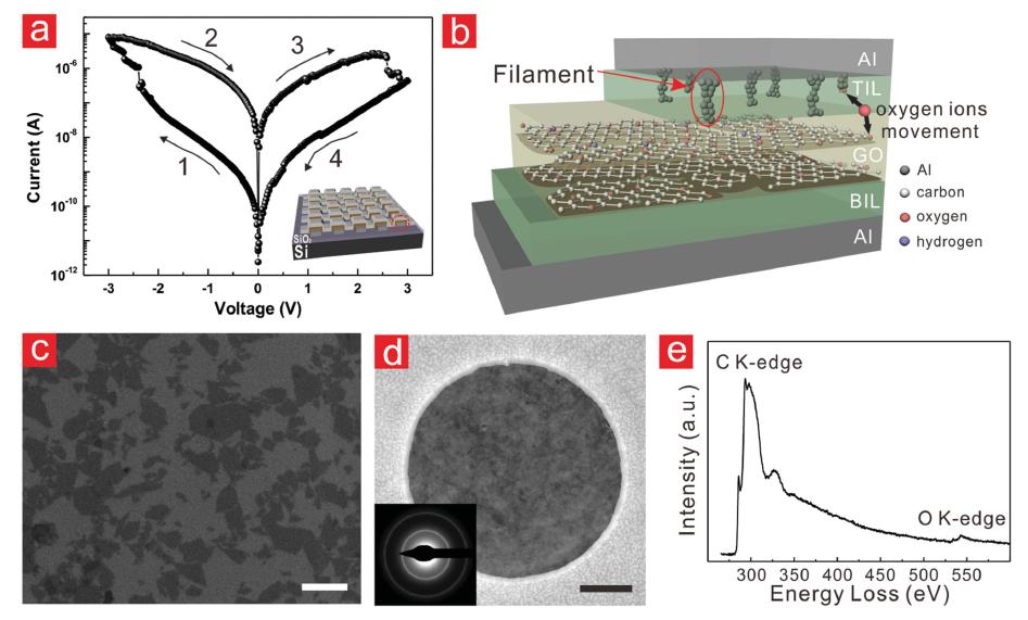
The operation principle of ‘Graphene Memory Device’ is discovered by the joint research team including Prof. Hu Young Jeong (UNIST Central Research Facility), Prof. Jeong Yong Lee (Department of Materials Science and Engineering, KAIST) and Prof. Sung-Yool Choi (Graphene Research Center, KAIST). They directly observed conducting nanofilaments in graphene-oxide-resistive switching memory and their research outcome was introduced on the world famous science journal, Advanced Functional Materials, on November 18, 2015 as the inside front cover.
Prof. Hu Young Jeong and his team discovered the performance principle of memory devices based on graphene-oxide (GO) thin films. They figured out how the electric current flows in GO even though it is an electric insulator. This observation was possible with a use of transmission electron microscope (TEM) which is established at UNIST. Considering the uniqueness and importance of this research outcome, the resistive random access memory (RRAM) will receive the attention as the next-generation nonvolatile memory device (NVM).
Memory is an electronic device where the information gets stored on computer. Recently, NVM became popular in the industry and research areas since it does not lose the information even if people turn the power off without storing the information they worked on. Current NVM devices use Silicon (Si), but there have been requests for smaller and thinner NVM.
Among next-generation NVM devices, RRAM has emerged as excellent candidate for overcoming the physical limitations of conventional charge based memory devices due to its simple structure, high density, low power consumption, and fast switching speed. In addition, RRAM with a use of GO thin films as the electric insulator became popular in various researches.
In this study, researchers put GO thin films which are less than a few hundred nanometers between metal electrodes. Generally, the electric current does not flow when electric resistance is too strong, but UNIST research team found out that electric current flows when it gets a certain pressure of electrostimulation. The transition between big electric resistance and small electric resistance is used in memory device development areas.
UNIST research team observed the two different devices that have different levels of electric resistance by using a TEM. Team members made the sample that they can observe devices by using Focused Ion Beam. Then, they observed the changes of electric resistance between the metal electrode and grapene-oxide film. Prof. Jeong’s research team decided to use Aluminum (Al) as the metal electrode among various metal electrodes on this research and they successfully observed the conducting nanofilaments in graphene-oxide-resistive switching memory.
Using a spherical-aberration-corrected TEM, they obtained cross-sectional TEM images of GO thin films sandwiched between two Al electrodes. The present study provides a basis for addressing the reaction phenomena between metal and nanoscale GO thin films and interpreting the bipolar resistive switching behaviors of AL/GO/Al memory devices.
Prof. Jeong says, “GO thin films are made of carbon and oxygen which are weak to the electron beam, so it is not easy to observe by using the general transmission electron microscope (TEM). Using a spherical-aberration-corrected transmission electron microscopic (TEM) which is established at UNIST made this research successful. Our research team discovered resistive change mechanism by observing the changes of GO thin films structurally and chemically.
This research was conducted by UNIST and KAIST and sponsored by the National Research Foundation, Institute for Basic Science, and Ministry of Science, ICT and Future Planning of Korea.


