The challenge to increase the micro-device integration density that determines semiconductor performance is ongoing. Professor Hyeon Suk Shin in the Department of Chemistry has developed a technology capable of synthesizing multiple layers of hexagonal boron nitride, the only 2D insulator, in the form of a single crystal thin film for the first time globally, charting the technological path of next-generation semiconductors.
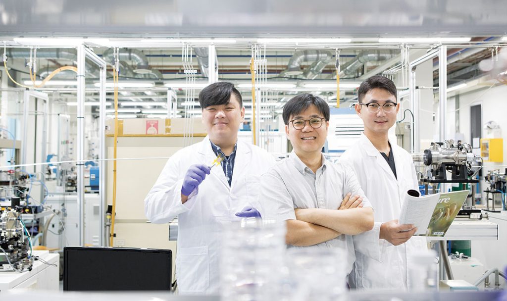
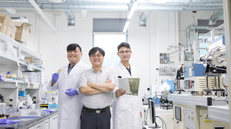
From the left are Hyeong Joon Kim (Ph.D. candidate), Professor Hyun Suk Shin, and Min Soo Kim (Ph.D. candidate).
Emergence of 2D Materials that Can Replace Silicon
Semiconductors have advanced at a breakneck speed over the past decades. The prediction of Gordon Moore that the integration density of microchips will double roughly every 24 months was nearly correct. Thus, it was called Moore’s Law, which represents the rapid technological growth in the semiconductor industry. However, it seems like Moore’s Law is becoming slowly obsolete when we see the current semiconductor development status.
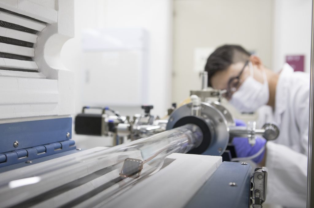
Min soo Kim (Ph.D. candidate) in the Department of Chemistry at UNIST.
One semiconductor chip contains billions of micro-devices (transistors). To increase the semiconductor performance, micro-devices should be smaller and thinner to fit more in one chip. However, silicon made of 3D materials has a fatal problem that degrades the semiconductor performance and life, such as short channel effect and charge scattering, which causes transistor damage due to current leakage and heating as it becomes smaller. This is because of the dangling bond, which is an incomplete chemical bond at the surface while processing the silicon surface. To solve this problem, the semiconductor industry has researched the use of 2D materials such as molybdenum disulfide (MoS2) instead of using 3D material silicon. The short channel effect and charge scattering, which are found when 3D materials are made smaller, do not occur in 2D materials because their composition atoms are connected in a plane form. Thanks to this, the micro-device integration density and semiconductor performance can keep improving using 2D materials.
World’s First Technology that Accelerates the Commercialization of 2D Insulators
There is one more problem to be solved when 2D materials are used as micro-devices instead of silicon. A wafer, a substrate on which micro-devices are laid, is also made of silicon. Thus, 2D material and wafer should be separated by an insulator to make semiconductors made of 2D materials to exhibit their functions. Here, the insulator should also be made of 2D materials. If the insulator is made of 3D materials, it cannot avoid adanglingbond. Hexagonal boron nitride (hBN) is a unique 2D insulator material, which is known to date, and can prevent semiconductor functional degradation problems, such as charge trap or charge scattering. Its molecular structure is similar to that of graphene, but its color is white, which is also called ‘white graphene.’ To use hBN as a 2D insulator, it should be synthesized into a single crystal structure where the entire crystal is regularly generated along a certain crystalline axis. Previously, there were cases of synthesis of a single crystal of hBN of which size can be commercialized. However the thickness of all synthesis was a layer of an atom, which could not function as an insulator.
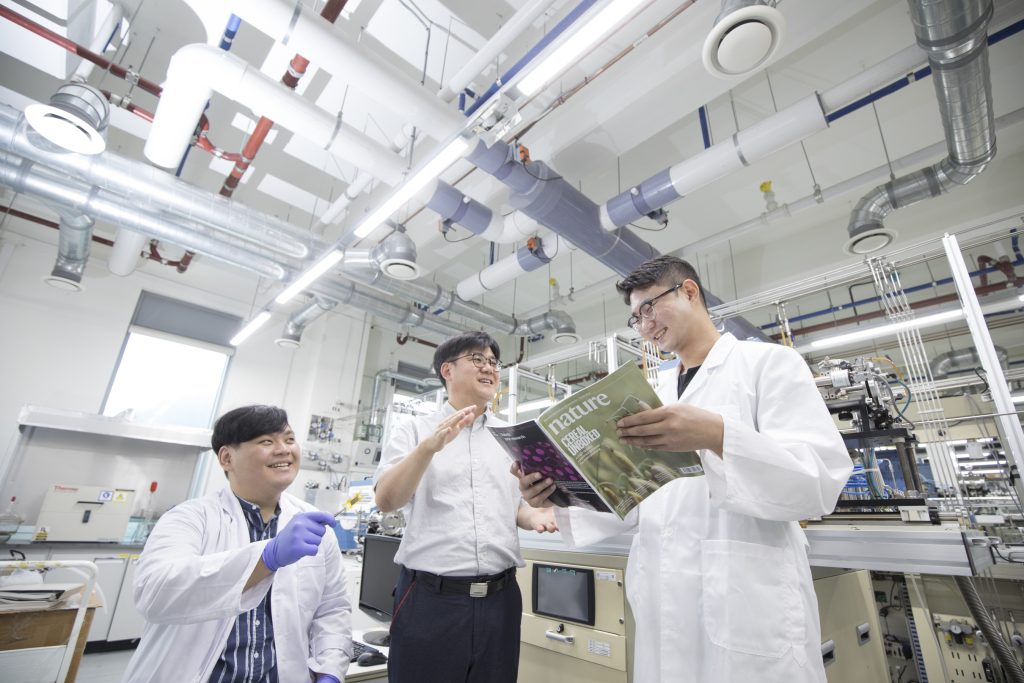
Professor Shin and his research team in the Department of Chemistry at UNIST.
The synthesis of hBN developed by Professor Hyeon Suk Shin and his research team in the Department of Chemistry at UNIST is a ground breaking technology that can stack single crystal hBN thin films in multiple layers. It is the world’s first synthesis technology that can make a single crystal hBN thin film at a preferred thickness while finely adjusting the concentration of the raw material on the nickel substrate. The paper titled 「Epitaxial single crystal hexagonal boron nitride multi-layers on Ni(111)」 that dealt with this research was published in the global academic journal Nature on June 2, 2022.
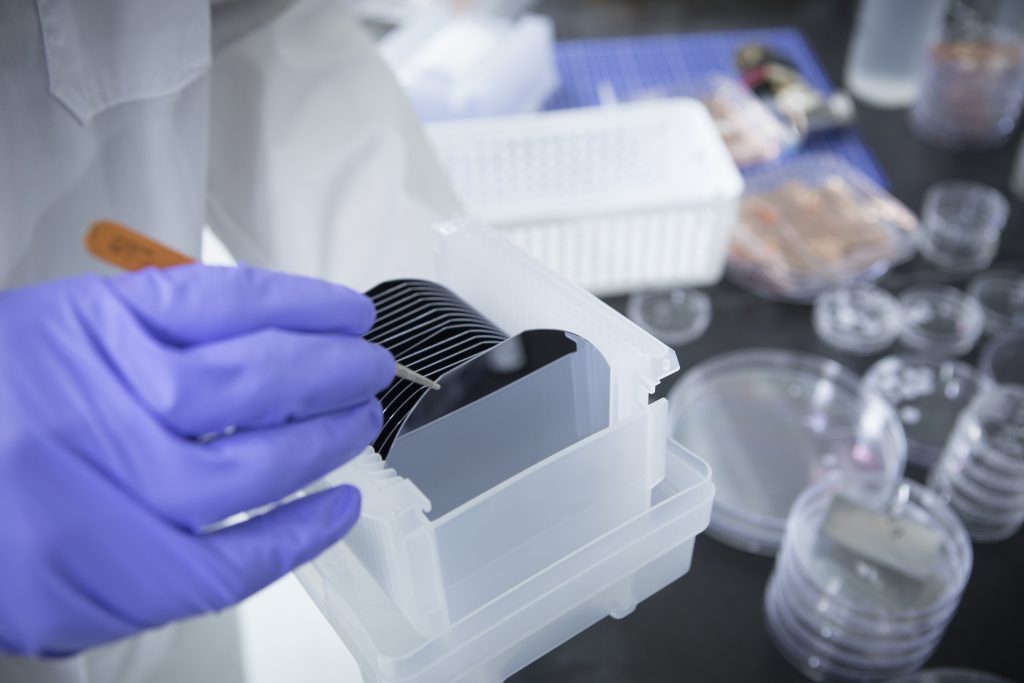
Contributing to Innovation in the Semiconductor Industry with Relentless Challenges
The synthesis method of single crystal multilayer hBN thin film developed by the team led by Professor Shin is not just a coincidence. Professor Shin has steadily conducted a study on the synthesis and application of hBN since 2012. In 2020, he disclosed that amorphous boron nitride, which is a kind of boron nitride, is an ultralow dielectric material that prevents the signal transmission delay in high-density semiconductors, and published this research achievement in the journal Nature.
“Amorphous boron nitride was discovered in 2018 when I studied hBN. Its dielectric constant was very low at 2.0 or lower so I found it could be used as a dielectric that blocked electrical interference when semiconductors were miniaturized during my research of two years. Since then, research and development have been conducted on the commercialization of amorphous boron nitride by many semiconductor companies. We expect that the synthesis method of single crystal multi-layer hBN thin film will play a significant role in improving semiconductor technology.”
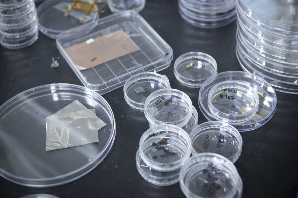
“We were successful in synthesizing single crystal hBN thin film at multiple layers, but for commercialization, we still need one more technology to be developed. That is a technology that transfers an hBN thin film synthesized on a nickel substrate onto a wafer without damage,” noted Professor Shin. The research team is now spurring research on this.
Professor Shin added, “Once this technology is developed, it can be used to transfer not only hBN thin films but also various 2D materials.” The team plans to widen its research even on application chemical areas using hBN in addition to the foundational research related to hBN. We hope their efforts will lead to the innovation of semiconductors.


