unist UNIST News Center UNIST News Center
KOREAN ENGLISH
  • HOME
  • Contents
    • All News
    • News
    • People
    • Community Contribution
    • Research
    • Decoding Fear’s Chemistry: Professor Haejin Yoon Wins HFSP Accelerator Grant 9 hours ago
    • UNIST 3D Printing Convergence Technology Center Hosts Successful Open House Event 2 days ago
    • New Study Unveils Atomic Disorder Strategy to Enhance Stability and Efficiency of High-Capacity Batteries 2 days ago
    View all
    • UNIST 3D Printing Convergence Technology Center Hosts Successful Open House Event 2 days ago
    • UNIST and KOSME Partner to Accelerate AI Transformation for SMEs in Southeastern Korea 1 week ago
    • New Quantum-Nano FAB at UNIST to Anchor Korea’s Open Quantum Research Ecosystem 2 weeks ago
    View all
    • Decoding Fear’s Chemistry: Professor Haejin Yoon Wins HFSP Accelerator Grant 9 hours ago
    • President Park’s Next Goal: AI Transformation of Manufacturing in Korea’s Southeastern Industrial Hub 4 weeks ago
    • Three UNIST Students Honored with 2026 Asan Foundation Biomedical Science Scholarship 4 weeks ago
    View all
    • UNIST and PKNU Sign MOU to Promote Educational Donations and Develop Joint STEM Programs in Gyeongsang Region 7 months ago
    • UNIST Connects with Community Through Spring Concert for Children with Disabilities 11 months ago
    • Flower Beds at UNIST Given A New Lease of Life! 5 years ago
    View all
    • New Study Unveils Atomic Disorder Strategy to Enhance Stability and Efficiency of High-Capacity Batteries 2 days ago
    • Innovative Recycling Method to Convert Waste PET into High-Quality Raw Materials and Clean Hydrogen 5 days ago
    • UNIST Achieves International Acclaim for Pioneering AI-Driven Music Learning Technology 5 days ago
    View all
  • For Journalists
    • For Journalists
    • UNIST at a Glance
  • About News Center
    • About News Center
    • News & Communications Team
Menu
  • HOME
  • Contents
    • All News
    • News
    • People
    • Community Contribution
    • Research
    • Decoding Fear’s Chemistry: Professor Haejin Yoon Wins HFSP Accelerator Grant 9 hours ago
    • UNIST 3D Printing Convergence Technology Center Hosts Successful Open House Event 2 days ago
    • New Study Unveils Atomic Disorder Strategy to Enhance Stability and Efficiency of High-Capacity Batteries 2 days ago
    View all
    • UNIST 3D Printing Convergence Technology Center Hosts Successful Open House Event 2 days ago
    • UNIST and KOSME Partner to Accelerate AI Transformation for SMEs in Southeastern Korea 1 week ago
    • New Quantum-Nano FAB at UNIST to Anchor Korea’s Open Quantum Research Ecosystem 2 weeks ago
    View all
    • Decoding Fear’s Chemistry: Professor Haejin Yoon Wins HFSP Accelerator Grant 9 hours ago
    • President Park’s Next Goal: AI Transformation of Manufacturing in Korea’s Southeastern Industrial Hub 4 weeks ago
    • Three UNIST Students Honored with 2026 Asan Foundation Biomedical Science Scholarship 4 weeks ago
    View all
    • UNIST and PKNU Sign MOU to Promote Educational Donations and Develop Joint STEM Programs in Gyeongsang Region 7 months ago
    • UNIST Connects with Community Through Spring Concert for Children with Disabilities 11 months ago
    • Flower Beds at UNIST Given A New Lease of Life! 5 years ago
    View all
    • New Study Unveils Atomic Disorder Strategy to Enhance Stability and Efficiency of High-Capacity Batteries 2 days ago
    • Innovative Recycling Method to Convert Waste PET into High-Quality Raw Materials and Clean Hydrogen 5 days ago
    • UNIST Achieves International Acclaim for Pioneering AI-Driven Music Learning Technology 5 days ago
    View all
  • For Journalists
    • For Journalists
    • UNIST at a Glance
  • About News Center
    • About News Center
    • News & Communications Team
Home All News Research Ultra-Large Single-crystal WS2 Monolayer
Ultra-Large Single-crystal WS2 Monolayer

Distinguished Professor Feng Ding and his colleagues from IBS CMCM at UNIST reported a new technique that opens up the possibility to replace silicon with 2D materials in semiconducting technology. Their findings have been published in the November 2021 issue of Nature Nanotechnology.

Ultra-Large Single-crystal WS2 Monolayer

Published in the November 2021 issue of Nature Nanotechnology, their findings open up the possibility to replace silicon with 2D materials in semiconducting technology.

Nov 19, 2021IBS Communications Team IBS
print

As silicon based semiconducting technology is approaching the limit of its performance, new materials that may replace or partially replace silicon in technology is highly desired. Recently, the emergence of graphene and other two-dimensional (2D) materials offers a new platform for building next generation semiconducting technology. Among them, transition metal dichalcogenides (TMDs), such as MoS2, WS2, MoSe2, WSe2, as most appealing 2D semiconductors.

A prerequisite of building ultra-large-scale high-performance semiconducting circuits is that the base materials must be a single-crystal of wafer-scale, just like the silicon wafer used today. Although great efforts have been dedicated to the growth of wafer-scale single-crystals of TMDs, the success was very limited until now.

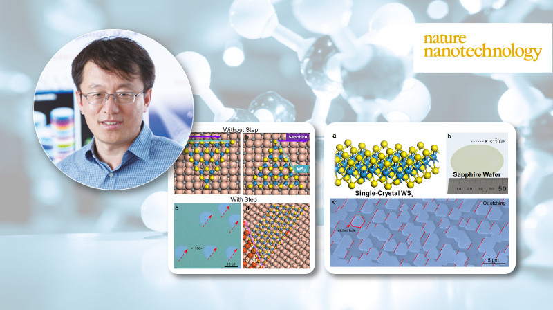
Distinguished Professor Feng Ding and his research team from the Center for Multidimensional CarbonMaterials (CMCM), within the Institute for Basic Science (IBS) at UNIST, in cooperation with researcher at Peking University (PKU), Beijing Institute of Technology, and Fudan University, reported the direct growth of 2-inch single-crystal WS2 monolayer films very recently. Besides the WS2, the research team also demonstrated the growth of single-crystal MoS2, WSe2, and MoSe2 in wafer scale as well.

Figure 1
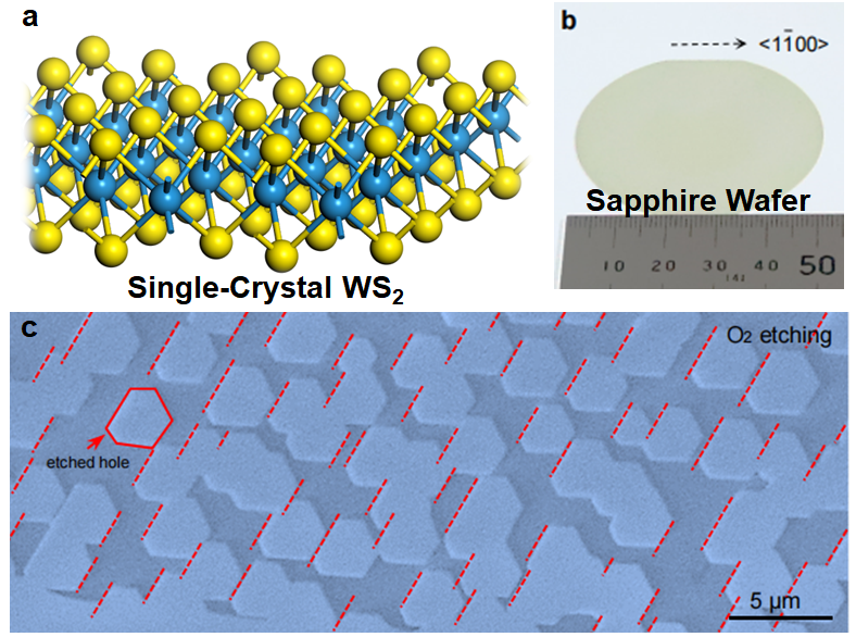
▲ Figure 1. a, Single-crystal WS2; b, Sapphire wafer used in industry is a single-crystal; c, Experimental images about the WS2 films on sapphire wafer after O2 etching.

The key technology of epitaxially grown a large sing-crystal is to ensure that all small single-crystal grown on a substrate are uniformly aligned. Because TMDs has non-centrosymmetric structure or the mirror image of a TMD with respect to an edge of it has opposite alignment, we must break such a symmetry by carefully design the substrate. Based on theoretical calculations, the authors proposed a mechanisms of “dual-coupling-guided epitaxy growth” for experimental design. The WS2-sapphire plane interaction as the first driving force, leading to two preferred antiparallel orientations of the WS2 islands. The coupling between WS2 and sapphire step-edge is the second driving force and it will break the degeneracy of the two antiparallel orientations. Then all the TMD single crystals grown on a substrate with step edges are all unidirectional aligned and finally, the coalescence of these small single-crystals leads to a large single-crystal of the same size of the substrate.

“This new dual-coupling epitaxy growth mechanism is new for controllable materials growth. In principle, it allows us realize to grow all 2D materials into large-area single crystals if proper substrate was found,” says Dr. Ting Cheng, the co-first author of the study. “We have considered how to choose proper substrates theoretically. First, the substrate should have a low symmetry and, secondly, more step edges are preferred,” emphasizes Professor  Ding, the corresponding author of the study.

Figure 2
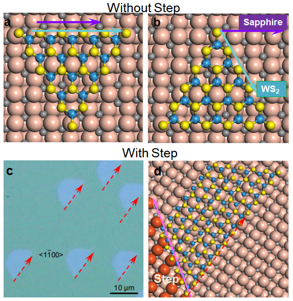
▲ Figure 2. a-b, Schematic diagrams of WS2 island on a flat a-plane sapphire surface, which has two preferred antiparallel orientations; c-d, The unidirectional alignment of WS2 island grown on vicinal a-plane sapphire with step.

“This is a major step forward in the area of 2D materials based device. As the successful growth of wafer-scale single-crystal 2D TMDs on insulators beyond graphene and hBN on transition metal substrates, our study provide the required keystone of 2D semiconductors in high-end applications of electronic and optical devices,” explains Professor Ding.

Feng Ding
Distinguished Professor, Dept. of Materials Science and Eng., UNIST
IBS Center for Multidimensional Carbon Materials (CMCM)

Dahee Carol Kim
IBS Communications Team
T: +82-42-878-8133
E:clitie620@ibs.re.kr

Story Source
Materials provided by the Institute of Basic Science.

Notes for Editors
This press release is made available courtesy of IBS Communications Team.

Journal Reference
Jinhuan Wang, Xiaozhi Xu, Ting Cheng, et al., “Dual-coupling-guided epitaxial growth of wafer-scale single-crystal WS2 monolayer on vicinal a-plane sapphire,” Nature Nanotechnology (2021). DOI: 10.1038/s41565-021-01004-0

Share 0
Tweet 0
Share 0
Share 0
Share 0
  • Previous

    Seven UNIST Faculty Named to Highly Cited Researchers 2021 List

  • Next

    UNIST’s AI Research Shines at Top-notch Academic Conferences!

author photo

Writer|IBS Communications Team |IBS

042-878-8114
webmaster@ibs.re.kr

Related Articles

  • New Study Unveils Atomic Disorder Strategy to Enhance Stability and Efficiency of High-Capacity Batteries

    New Study Unveils Atomic Disorder Strategy to Enhance Stability and Efficiency of High-Capacity Batteries

    Mar 23, 2026
  • Innovative Recycling Method to Convert Waste PET into High-Quality Raw Materials and Clean Hydrogen

    Innovative Recycling Method to Convert Waste PET into High-Quality Raw Materials and Clean Hydrogen

    Mar 20, 2026
  • UNIST Achieves International Acclaim for Pioneering AI-Driven Music Learning Technology

    UNIST Achieves International Acclaim for Pioneering AI-Driven Music Learning Technology

    Mar 20, 2026
  • New Study Unveils High-Performance LFP Cathodes to Extend Electric Vehicle Range

    New Study Unveils High-Performance LFP Cathodes to Extend Electric Vehicle Range

    Mar 19, 2026

Popular

  • UNIST 3D Printing Convergence Technology Center Hosts Successful Open House Event

    UNIST 3D Printing Convergence Technology Cente..

    Mar 24, 2026
  • New Study Unveils Atomic Disorder Strategy to Enhance Stability and Efficiency of High-Capacity Batteries

    New Study Unveils Atomic Disorder Strategy to ..

    Mar 23, 2026
  • Innovative Recycling Method to Convert Waste PET into High-Quality Raw Materials and Clean Hydrogen

    Innovative Recycling Method to Convert Waste P..

    Mar 20, 2026

UNIST E-Newsletters

Sign up today to receive a copy of the UNIST e-newsletter

<Personal Information Processing Consent Form>
UNIST wishes to obtain consent from Newsletter subscribers to the collection and processing of their personal information. Please read this document in its entirety before giving consent (select each blank as appropriate).

1. Items to be collected : e-mail address
2. Purposes of collection and use : to provide Newsletter service
3. Period of holding and use : until your cancelation
4. You have the right to refuse consent. However, you may not be provided with the aforementioned services due to rejection.
I give my consent for all personal information to be processed for the purposes described in this document and understand that I can withdraw my consent at any time.
  • UNIST Daily
  • UNIST Newsletter
  • For Journalists
logo
50 UNIST-gil, Ulsan 44919, Republic of Korea
Phone : +82 52 217 0114 /Admissions : +82 52 217 1120
  • Contents
    • News
    • People
    • Research
    • Photo & Video
  • For Journalists
    • UNIST at a Glance
  • About News Center
    • About News Center
    • UNIST Newsletter
    • Send Your Story Ideas
    • News & Communications Team