
A research team, affiliated with UNIST has unveiled a groundbreaking material to tackle a critical challenge in shrinking semiconductor circuits.
Led by Professor Soo-Hyun Kim in the Department of Materials Science and Engineering at UNIST, the team announced the successful development of a novel ruthenium (Ru) precursor and an innovative atomic layer deposition (ALD) process utilizing this material. Ru, a promising metal for next-generation chip wiring, offers better conductivity at nanoscale dimensions and eliminates the need for additional diffusion barrier layers required by copper (Cu), simplifying manufacturing and improving reliability.
The new precursor exhibits remarkable thermal stability up to 400 °C, enabling high-temperature ALD processes that produce dense, high-quality Ru films without degradation. This stability allows for faster, more efficient deposition, overcoming the limitations of existing Ru precursors that typically break down at elevated temperatures. The process deposits an ultra-thin, precise Ru layer, achieving a growth rate of approximately 1.28 Å per cycle—almost double that of previous methods—and requires only about 8 cycles to form a conformal coating.
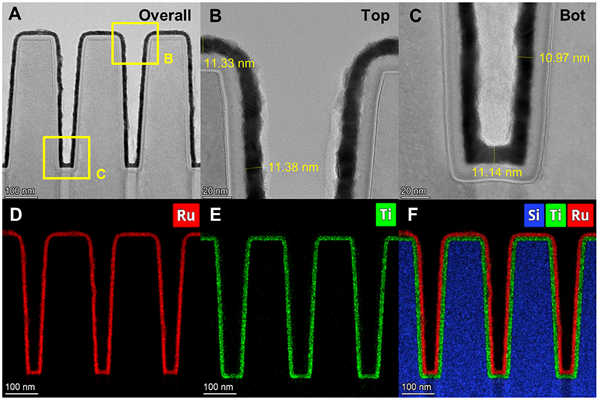 Figure 1. Advanced aberration-corrected microstructure analysis, step coverage, and elemental confirmation of ALD-Ru thin films. Cross-sectional view transmission electron microscopy (XTEM) of A) overall, B) top of the trench, and C) bottom of the trench. Elemental mapping quantification for D) Ru, E) Ti, F) full Ru, Ti, and Si.
Films grown using this precursor demonstrate excellent electrical properties, with resistivity values as low as 10.6 μΩ·cm—approaching bulk Ru’s 7.4 μΩ·cm—even without additional heat treatment. The coatings also exhibit over 95% conformality, effectively covering complex 3D structures such as narrow trenches, which is vital for advanced memory and logic devices.
Additionally, the process shows excellent substrate selectivity, depositing ruthenium only on targeted areas and avoiding nucleation on SiO₂—even after 1000 cycles at 300 °C—supporting area-specific integration in complex architectures. Microstructural analyses—including EBSD, advanced aberration-corrected UHR-TEM/STEM, FS–MS modeling, and MLIP-based energy calculations—reveal improvements in crystallinity, grain growth, and the formation of low-energy grain boundaries that reduce electron scattering, further enhancing electrical performance.
Compared to conventional Ru-ALD processes plagued by low growth rates, long incubation times, and thermal instability, this new precursor provides a scalable, efficient solution for low-resistance, barrierless metal interconnects in advanced semiconductor nodes.
“Achieving low-resistance wiring with high uniformity and process efficiency at nanoscale dimensions is crucial,” noted Professor Kim. “Our development offers a significant step toward more reliable and high-performance chip manufacturing.”
The findings of this research have been published in the online version of Advanced Science on November 23, 2025. This study has been carried out in collaboration with Tanaka Precious Metal Technologies Co., Ltd., a Japanese company specializing in precious metals. It has been also supported by the Ministry of Trade, Industry and Energy (MOTIE) through the Industrial Strategic Technology Program, highlighting its potential impact on industry.
Journal Reference
Hideaki Nakatsubo, Debananda Mohapatra, Eun-Soo Lee, et al., “Small and Simple Molecular Structure Based Thermally Stable Ruthenium Precursor in Advancing Ruthenium ALD Process for Scaled Interconnect Metallization,” Adv. Sci., (2025).


