《Editor’s Note: This research has gained much attention from academia since it was introduced in the February 2019 issue of Nature Nanotechnology. Click HERE to read the article. | 2019.02.19.》
A new study, affiliated with UNIST has introduced a novel technology, capable of fabricating highly ordered arrays of graphene quantum dot (GQD). The new technology is expected to pave the way for many other types of devices and physical phenomena to be studied.
This breakthrough has been led by Professor Hyeon Suk Shin in the School of Natural Science at UNIST. In their study, the research team demonstrated a novel way of synthesizing GQDs, embedded inside the hexagonal boron nitride (hBN) matrix. Thus, they demonstrated simultaneous use of in-plane and van der Waals heterostructures to build vertical single electron tunnelling transistors. Their findings have been published in the online edition of Nature Communications on January 16, 2018.
Graphene quantum dots (GQDs) have received much research attention, due to their unique fluorescence emission propertie. Thus, they have emerged as an attractive tool for many applications, from cutting-edge displays to medical imaging. Besides that, they are applicable to materials for the next-generation quantum information communication technology, capable of processing information with low electricity use.
Until now, GQDs are prepared through simple chemical exfoliation method, in which it exfoliates graphene sheets from bulk graphite. Such method has made impossible the production of GQDs of desired size, thereby This not only invites impurities at the edge of GQDs, but also significantly impedes the flow of electrons. This hinders GQDs to exhibit their unique optical and electrical properties.

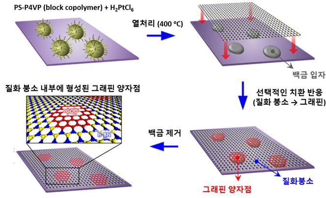
The fabrication steps of GQD-hBN in-plane heterostructure based on hBN to graphene conversion catalysed by Pt NPs.
Professor Shin and his research team succeeded in demonstrating novel way of removing the impurities at the edge of GQDs and adjusting the size of GQDs, as desired. The growth of in-plane GQD-hBN heterostructure was achieved on a SiO2 substrate covered by an array of platinum (Pt) nanoparticles (NP), as illustrated in figure above. Then, this was treated with heat in methane (CH4) gas. As a result, the size of GQDs was decided according to the size of Pt particles, thereby generating highly-ordered GQDs inside the matrix of hexagonal boron nitride.
“Since graphene and h-BN are similar in structure, it was possible to grow GQDs inside the matrix of h-BN ,” says Gwangwoo Kim in the School of Energy and Chemical Engineering at UNIST, the first author of the study. “The growth of GQDs embedded in the hBN sheet are chemically bonded to BN, thus minimizing impurities.”

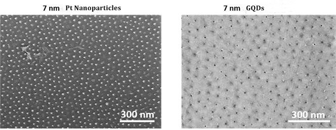
The SEM images of highly-ordered Pt nanoparticles and graphene quantum dots (GQDs).
Using the technology, the team fabricated arrays of highly-ordered uniform GQDs, and thus was able to adjust their sizes from 7 to 13 nm. They also succeeded in implementing vertical single electron tunnelling transistors that minimizes impurities to move electrons stably.
“The graphene quantum-dot-based single-electron transistor will be applied to electronic devices that operate through fast information processing at low power,” says Professor Shin.
This study has been jointly conducted by Professor Byeong-Hyeok Sohn from Seoul National University and Professor Konstantin Novoselov from the University of Manchester in UK. It has been supported by IBS Center for Multidimensional Carbon Materials (CMCM) and the research grant from the Center for Advanced Soft Electronics under the Global Frontier Research Program through the National Research Foundation by the Korean Ministry of Science.
Journal Reference
Gwangwoo Kim et al., “Planar and van der Waals heterostructures for vertical tunnelling single electron transistors,” Nature Commnucations, (2019).


