A research team, led by Professor Oh-Hoon Kwon in the Department of Chemistry at UNIST has reported that they had succeeded in forming fine patterns with nanometer-level accuracy on black phosphorus, a semiconductor material, using femtosecond (10-15 seconds) lasers and creating various types of nanostructures. It also presented a theoretical background that can explain the physical reason for the formation of nano-patterns and the strong interaction between light and materials underlying them by observing the entire process directly in real and time space through a transmission electron microscope.
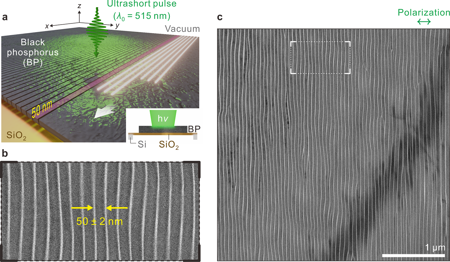
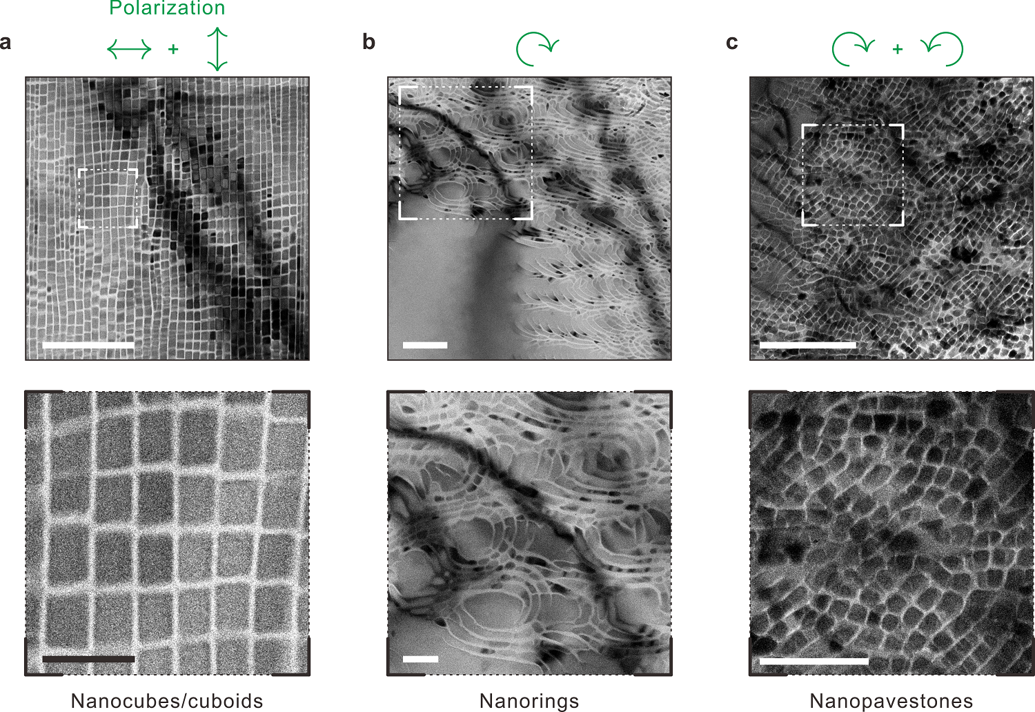
The research team instantaneously irradiated a black phosphorus sample with light of 515 nm wavelength corresponding to visible light to create a nanoribbon array with a width equal to one tenth of the wavelength of light and an interval equal to one hundredth of the wavelength. This is the resolution reaching the minimum line width of the pattern that can be expressed by the extreme ultraviolet exposure device. In particular, depending on the polarization of light exposed regardless of the crystal structure of the black phosphorus sample, the direction of ribbon formation or various types of nanostructures such as cubes and rings can be freely manufactured. This is different from synthesis methods that can make only nanostructures having a specific crystal direction.

Figure 1. Laser-induced in situ nanosculpting BP. (a) Schematic illustration of wide-field nanosculpting BP with femtosecond-pulsed light. Incident light induces self-organized optical fields in BP, resulting in highly regular nanostructures over micrometer area by structured periodic ablation with a width of approximately 50 nm. Inset: side view of experimental layout. (b) In-situ wide-field nanostructuring of black phosphorus. (c) Low-magnification bright-field TEM image of the BP nanoribbon array at marked position (square) in panel c. Orientation (grating vector) of the array is parallel to light polarization (denoted above panel). Crystalline axes (AC and ZZ) are denoted. Scale bar: 1 μm. Inset: fast-Fourier transform of array; scale bar: 50 μm–1.
Electron-beam lithography (EBL), which is currently the most widely used in device micro-processes, has high resolution and precision processing capabilities. However, it takes a lot of time and money because it goes through a number of processes. In addition, there is a disadvantage in that the resolution and the amount of information processing are inversely proportional in the process of scanning the electron beam on the substrate. On the other hand, the research team’s wide-field photolithography technique has the advantage of being able to process an area 1,000 times the resolution at once without requiring a pre-process process.

Figure 2. BP nanosculptures. (a–c) High- and low-magnification bright-field TEM images of nanosculptures.
The research team proved that the reason why fine nano patterns could be formed on black phosphorus using light was because of the formation of “soliton” by the modulation instability of light. When light undergoes disturbance motion in a non-linear medium such as black phosphorus, it can form a specific wave that maintains the waveform and velocity without energy loss, which is soliton. In other words, black phosphorus interacts with the irradiated laser light to generate solitons, and a pattern was created when phosphorus atoms were emitted along the floor of the wave with increased energy.
The theoretical and computational analysis of this study has been jointly conducted by Professor Q-Han Park in the Department of Physics at Korea University, and a research team of Professor Kwanpyo Kim in the Department of Physics at Yonsei University. Published in the March 2023 issue of Nano Letters, this study has been carried out with the support of the Samsung Science and Technology Foundation.
Journal Reference
Ye-Jin Kim, Yangjin Lee, WonJae Choi, et al., “Tailoring Two-Dimensional Matter Using Strong Light–Matter Interactions,” Nano Letters, (2023).


