A joint research team, affiliated with UNIST has recently unveiled a novel method, capable of controlling the brightness and wavelength of quantum dots (QDs), used in display applications, such as TVs. Published in the journal ACS Nano, this breakthrough has been led by Professor Kyoung-Duck Park in the Department of Physics at UNIST, in collaboration with Professor Sohee Jeong in the Department of Energy Science from Sungkyunkwan University (SKKU).

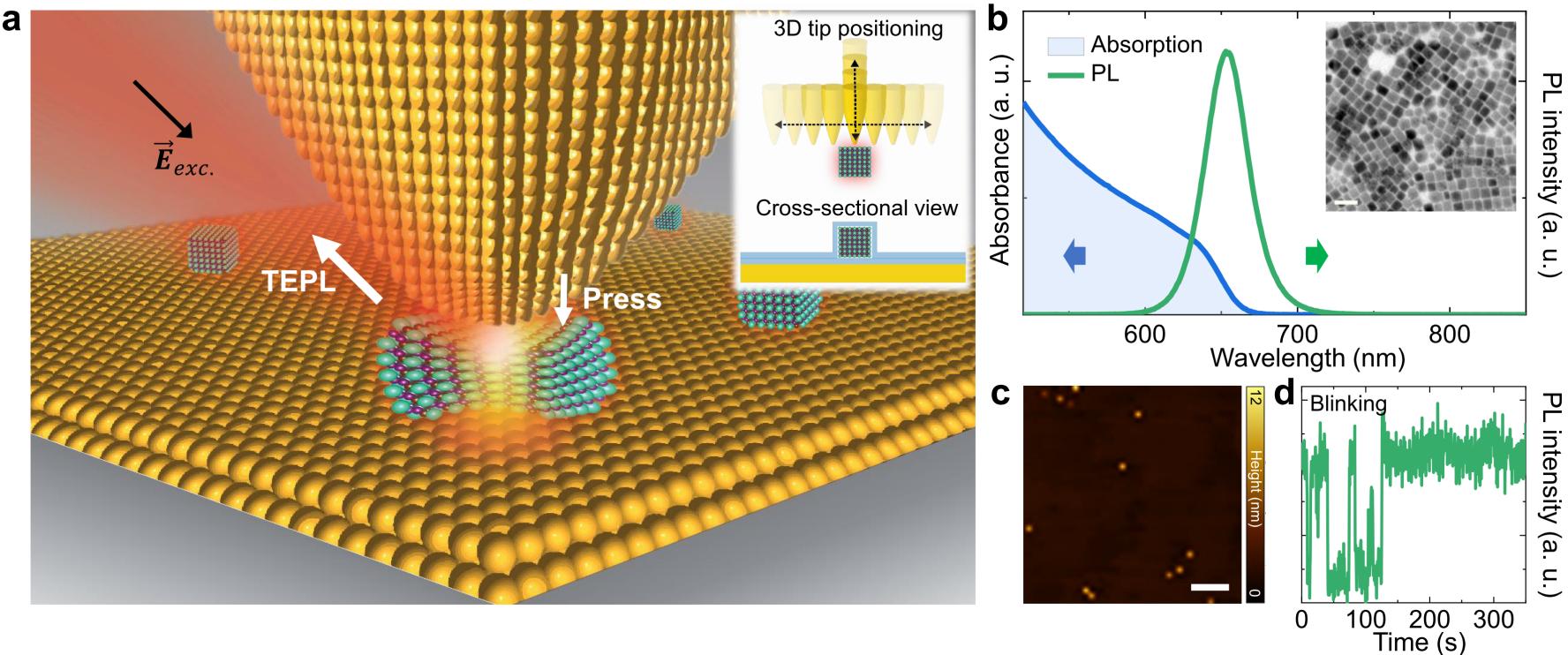
Figure 1. Schematic of experimental setup and characterization of single pQDs.
In this work, the research team demonstrated the tip-induced dynamic control of strain, bandgap, and quantum yield of single CsPbBrxI3–x pQDs by using a controllable plasmonic nanocavity combined with tip-enhanced photoluminescence (TEPL) spectroscopy.
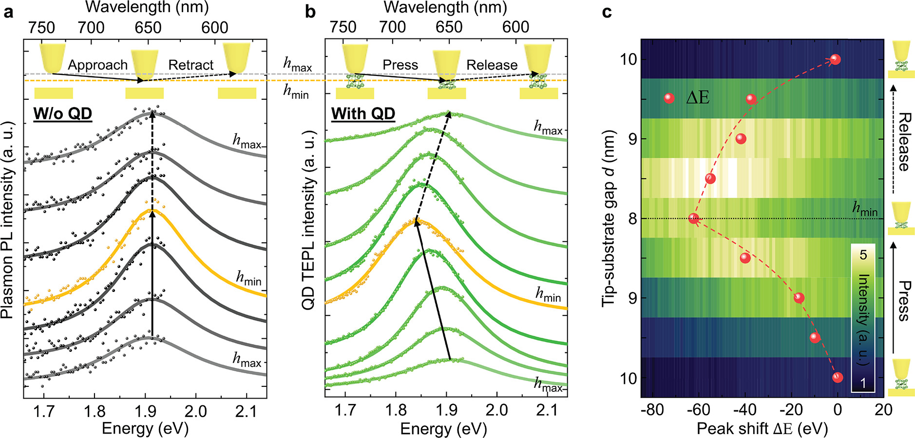
Through experiments, the research team discovered that single CsPbBrxI3–x pQDs were clearly resolved through hyperspectral TEPL imaging with ∼10 nm spatial resolution. The plasmonic tip then directly applied pressure to a single pQD to facilitate a bandgap shift up to ∼62 meV with Purcell-enhanced PL increase as high as ∼105 for the strain-induced pQD. Furthermore, by systematically modulating the tip-induced compressive strain of a single pQD, researchers achieved dynamical bandgap engineering in a reversible manner. In addition, they facilitate the quantum dot coupling for a pQD ensemble with ∼0.8 GPa tip pressure at the nanoscale estimated theoretically.
This tip-induced nanoengineering approach with local pressure of GPa order not only provides an in-depth understanding of the optical properties of metal halide perovskite pQDs and their coupling nature but also offers a practical way to tune the mechanical and electronic properties at the single-pQD level for potential applications in ultra-compact nano-optoelectronic devices, noted the research team.
Specifically, the research team anticipates that this dynamical single-dot manipulation will enable the tunable nano-LEDs, realizing ultra-high definition display with high efficiency. “In addition, extremely high tip-induced local pressure will allow pressure-induced recrystallization and phase transition at the few-nanometer-length scale to further improve the grain quality and optical properties of 2D perovskite ensembles as a post-fabrication process,” noted the research team. “Furthermore, the extrinsically modified physical properties of pQDs by the plasmonic cavity, e.g., reduced nonradiative recombination, modulation of carrier dynamics and PL lifetime, and enhanced radiative decay rate, can significantly improve the efficiency of perovskite photovoltaics.”

Figure 2. Strain, bandgap, and PLQY engineering of a single pQD.
Meanwhile, the 10 nm pQDs were produced by Professor Sohee Jeong from Sungkyunkwan University and Dr. Woo Joo-young from the Korea Institute of Industrial Technology (KITECH). Professor Mun Seok Jeong from Hanyang University also participated in the analysis of the unique properties of QDs, as well as the room temperature stabilization of QDs. In addition, the theoretical calculation for the physical interpretation of research results was led by Professor Yong-Hyun Kim from KAIST.
This study was made available in the online version of ACS Nanoi, ahead of its publication on May 25, 2021. Patent applications for the source technology with regard to controlling the properties of single QDs have been filed under the PCT. This study has been supported by KITECH, UNIST, and the National Research Foundation (NRF) of Korea funded by the Ministry of Science and ICT (MSIT).
Journal Reference
Hyeongwoo Lee, Ju Young Woo, Dae Young Park, et al., “Tip-Induced Strain Engineering of a Single Metal Halide Perovskite Quantum Dot,” ACS Nano, (2021).


