Graphene has become a rich topic to explore by many materials scientists and engineers, as well as chemists and physicists worldwide due to its exceptional properties. However, the main issue that scientists are faced with is the obstacle of improving the performance of the existing silicon used in semiconductors. Because graphene is a conductor without a band gap, it is impossible to control the electric current. This makes the material difficult to be used as a semiconductor. As a result, researchers have been hard at work to develop materials to replace silicon for years now.
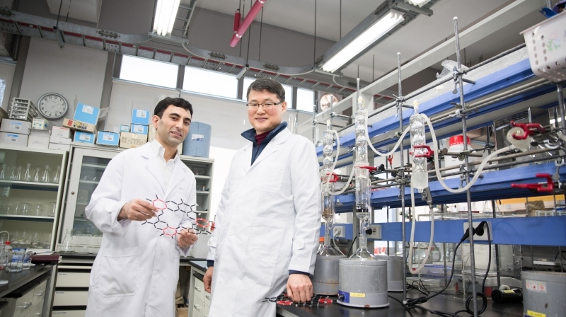
On March 6, a team of scientists, led by Prof. Jong-Beom Baek (School of Energy and Chemical Engineering) announced that they have successfully developed a technique to synthesize a new multifunctional 2D ordered crystal structure, designated as C2N-h2D crystal that is superior to graphene in electrical characteristics.
In this study, field-effect transistors (FETs) were fabricated using C2N-h2D crystals as the active layer in order to illustrate the electrical properties. According to Prof. Baek, this structure proves to be 100 times better than the existing silicon semiconductors in a ratio of electric current in semiconductors. An increase in the ratio helps control the flow of the elctric charge in semiconductors, which makes it possible to make high-performance semiconductors.
Prof. Baek’s says, “There are many known difficulties involved in the synthesis of graphene and h-BN, and the synthesis of the C2N-h2D crystals is a simple and highly efficient method for the formation of a fused aromatic 2D network structure.”
This newly-developed 2D crystal structure is composed of six benzene rings connected with nitrogen atoms in a larger hexagonal shape and can be used in semiconductor devices, as well as for energy storage purposes.
According to Prof. Beak’s team, “This unique material will open new opportunities in materials science and technology and thus broaden the horizon of applications in electronics, sensors, catalysis and many more research areas.”
The study was funded by Korea’s Ministry of Science, ICT and Future Planning, under the Project to Nurture Leading Creative Researching Experts Program. The research findings were appeared online in Nature Communications on March 6, 2015.
Journal Reference: Javeed Mahmood, Eun Kwang Lee, Minbok Jung, Dongbin Shin, In-Yup Jeon, Sun-Min Jung, Hyum-Jung Choi, Jeong-Min Seo, Seo-Yoon Bae, So-Dam Sohn, Moejung Park, Joon Hak Oh, Hyung-Joon Shin, Jong-Beom Baek, “Nitrogenated holey two-dimensional structures.” Nature Communications (6), Article Number: 6486.


