The formation of cracks is thought of as an unavoidable, unpleasant phenomenon because people believe that it is impossible to prevent cracking from all various forces. In recent years, scientists have demonstrated the ways to control fracture progression, thereby enabling researchers to manufacture high-resolution microscopic patterns of cracks.
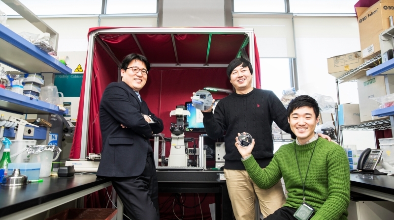
On March 5, a research team led by Prof. Tae-Sung Kim (School of Mechanical and Nuclear Engineering) announced that they have successfully developed a technology that can not only control the spread of nanometre-sized cracks, but also create well-controlled nanopatterns in any desired shape without using expensive equipment.
Photolithography and Electron-Beam Lithography
Current techniques, used in micro and nanofabrication technology are based on lithography and etching. Photolithography, which is a form of lithography, is a process that uses UV light to create high-resolution patterns of holes, channels or more complex structures in light-responding materials on top of a silicon wafer. In this process, the wafer is coated with resist, covered with a mask with an engraved pattern, and exposed to a focused beam of UV light. Then, during the etching process, the areas that are not protected by the resist are selectively removed, imprinting the patterns onto the wafer.
Although Photolithography is the most widely used technique and it allows the patterning of a desired design onto a silicon wafer, it has the disadvantage of fabricating patterns at micro level only. Therefore, as a solution, Electron-Beam Lithography (EBL) is employed to create the smallest components on silicon substrates. Today, EBL is the most effective method of creating patterns on substrates, yet the most expensive and time-consuming process.
The Ultimate Manufacturing Solution
UNIST research team was able to find a faster and cheaper way to engrave nanometer-sized patterns on the surface of a silicon wafer using the existing manufacturing process. The most notable characteristic of this study is that with this new approach, researchers can freely control the length and the direction of cracks, thereby creating more complex structures, such as circles and triangles at the microscopic level. Moreover, with the development of this technique, researchers can now produce nano-scale patterns, which used to take 10 days within only 30 minutes.
Prof. Kim states, “This new technique, produced by controlling cracks is a new alternative to existing complex and inefficient nanomanufacturing technology.” He continues by saying that, “I believe that this new approach will open a whole new chapter in nano technology, including machinery, electricity, electronics, bio-engineering, chemistry, environment, and energy, in addition to the materials industry.”
This research was funded by the National Research Foundation, under the Project to Support Leading Researchers and the findings were appeared online in Nature Communications on February 18, 2015.
Journal Reference: Minseok Kim, Dogyeong Ha, Taesung Kim, “Cracking-assisted photolithography for mixed-scale patterning and nanofluidic applications.” Nature Communications (6), Article Number: 6247.


