A research team, affiliated with UNIST has made a significant breakthrough in overcoming one of the most persistent challenges hindering the commercialization of two-dimensional (2D) semiconductor materials—contact resistance. Their findings shed light on the longstanding discrepancy between theoretical models and experimental results concerning the energy barriers that impede electron flow at contact interfaces, paving the way for more accurate performance predictions and faster development of ultra-scaled 2D semiconductor chips.
Led by Professors Changwook Jeong and Soon-Yong Kwon from the Graduate School of Semiconductor Materials and Devices Engineering at UNIST, the team identified the root cause behind the mismatch between existing theoretical models and experimental results concerning the energy barriers formed at the interface between 2D semiconductors and semi-metallic materials, known as bialkali metals. They also proposed a new predictive formula that more accurately reflects the complex physics at play in these interfaces.
As the semiconductor industry moves toward chips with feature sizes below ten nanometers, 2D materials have garnered increasing attention as promising alternatives to silicon, thanks to their atomic-scale thickness and exceptional electronic properties. However, integrating these materials with conventional metallic electrodes often results in high contact resistance, primarily due to the Schottky barrier—a potential energy obstacle that electrons must overcome to transition from metal to semiconductor.
While bialkali metals have been experimentally regarded as promising candidates for reducing these barriers, their reliability has been questioned. Conventional theoretical calculations tend to predict higher energy barriers than what is observed in practice, leading to uncertainty about their practical viability.
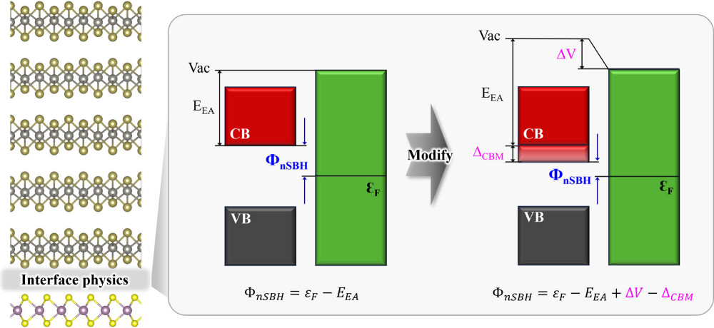
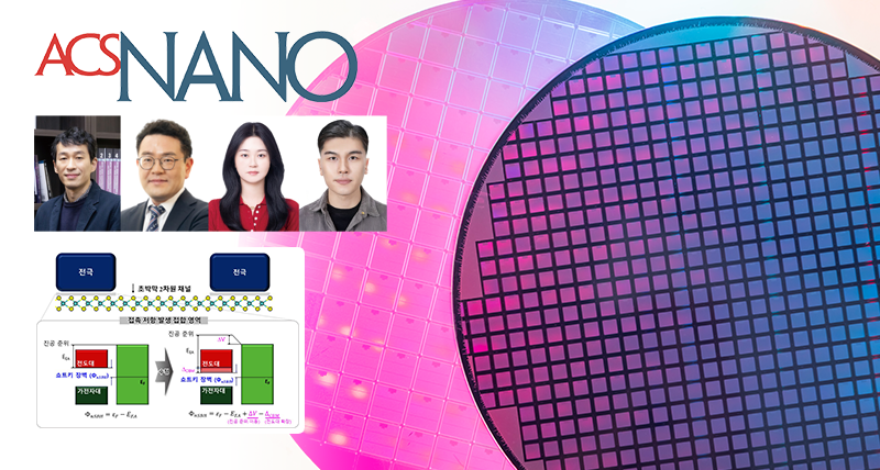
Figure 1. Schematic image illustrating the overall study of the research.
The research revealed that this inconsistency originates from a phenomenon called, Conduction Band Extension within molybdenum disulfide (MoS₂), a representative 2D semiconductor. When the metal contact approaches the semiconductor at specific angles, the conduction pathways within the material expand, effectively lowering the energy barrier and facilitating electron movement across the interface.
Building on this insight, the team developed an improved predictive formula that incorporates both the conduction band extension effect and the often-overlooked Vacuum Level Shift—a minor yet impactful factor that can significantly influence the barrier height in ultrathin 2D materials.
This revised model successfully reproduces experimental results that previously defied explanation by traditional approaches such as the Schottky-Mott rule, thereby providing a more reliable theoretical framework for interface physics in 2D nanoelectronics.
Professor Jeong remarked, “Our findings fundamentally clarify the mechanisms behind energy barrier formation at the interfaces of 2D semiconductors and semi-metals, which traditional theories failed to explain. By establishing a more accurate and comprehensive model, we can more efficiently identify optimal material combinations and device architectures, ultimately accelerating the development of next-generation semiconductor technologies.”
The findings of this research have been published in ACS Nano on November 4, 2025.
Journal Reference
Juwon Han, Hyeonwoo Lee, Youseung Lee, et al., “Contact Physics in 2D Nanoelectronics: Comparative Study of Type-II Weyl and Dirac Semimetals,” ACS Nano, (2025).


