A team of researchers, affiliated with UNIST has developed a metamaterial that improves the sensitivity of infrared absorption spectroscopy more than 100 times. The special material can be used in the creation of ultra-sensitive infrared sensors for the detection of biomolecules and harmful substances. It is very affordable and easy to make.
This breakthrough has been jointly carried out by Professor Jongwon Lee in the Department of Electrical Engineering at UNIST and Dr. Joo-Yun Jung from the Korea Institute of Machinery and Materials (KMMM).

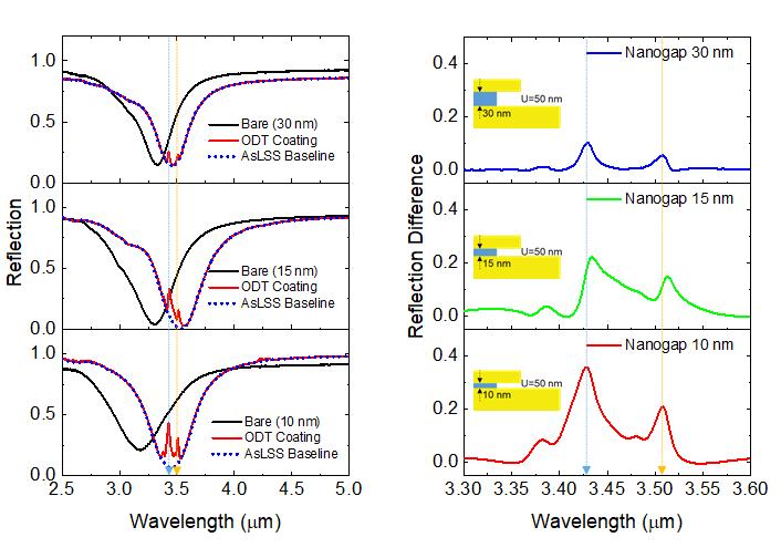
Figure 1. Left) Measured reflection spectra of the MA with 30 nm (top panel), 15 nm (middle panel), and 10 nm (bottom panel) vertical nanogaps before (black) and after (red) ODT coating. The blue-dotted curve indicates the numerically calculated baseline using the AsLSS algorithm, and the blue and orange vertical lines indicate the two vibrational absorption peaks of the ODT molecule. Right) Measured reflection difference SEIRA signal for the MA with 30 nm (top panel), 15 nm (middle panel), and 10 nm (bottom panel) vertical nanogap structures.
A metamaterial is a synthetic material that is engineered to have a property that is not found in naturally occurring materials. The special material is normally made of microscopic-sized assemblies of multiple materials including metals and plastics arranged in repeating patterns. It is used to manipulate electromagnetic waves by blocking, absorbing, strengthening, or bending waves. Any form of light can be described as an electromagnetic wave.
Infrared spectroscopy is a test method used to verify the type of substances on a surface by radiating infrared light onto a material and calculating the strength of the reflected light. Each substance has its own unique light-absorbing characteristics so that researchers can recognize the types. However, if there is only a tiny trace of a substance, there is hardly any difference in the strength of the reflected light, making it harder to detect.

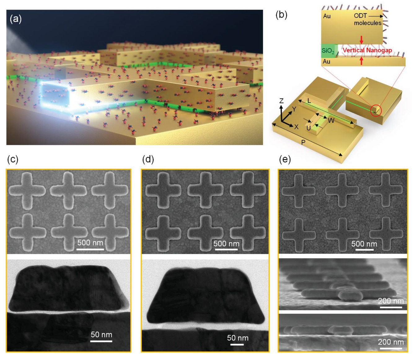
Figure 2. Schematic images of a) the MA with a vertical nanogap and its unit cell structure and b) zoomed-in image of the vertical nanocap edge portion of the MA with ODT monolayer. Top view of SEM images (top panel) and cross-sectional TEM images (bottom panel) of the processed MAs with c) 10 nm and d) 15 nm vertical nanogaps. e) Top view (top panel), tilted view (middle panel), and cross-sectional (bottom panel) view of SEM images of the processed MA with a 30 nm vertical nanogap.
In the study, the research team developed a highly effective metamaterial that can be easily mass-produced for a low price. It was created using crisscross layers of nanoantennae in a metal-insulator-metal configuration to have vertical nano-sized gaps of a smaller size than the infrared wavelength. Each layer is 10-nanometer thick.
“The proposed metamaterial achieved a record-high difference of 36 percent in our demonstration on a monolayer with a thickness of 2.8 nanometers. This is the best record achieved to date among monolayer detection experiments,” UNIST researcher Hwang In-yong said. Conventional metamaterials require expensive high-resolution lithography machines to produce microstructures on the material’s surfaces, but KIMM’s production stages involve affordable nanoimprint lithography and dry-etching processes to cut manufacturing costs.
This study was made available, ahead of its publication, in the online version of Small Methods on May 13, 2021. It was also selected as one of the hot topics in interface science research.
Journal Reference
Inyong Hwang, Mingyun Kim, Jaeyeon Yu, et al., “Ultrasensitive Molecule Detection Based on Infrared Metamaterial Absorber with Vertical Nanogap,” Small Methods, (2021).


