Quantum computing and quantum communication are two of the next-generation information processing technologies with high computational speed and high security. The technique to create and control the quantum emitters is at the core of such quantum information technology.
A research team, led by Professor Je-Hyung Kim in the School of Natural Sciences at UNIST has succeeded in simultaneously controlling the position and frequency of the quantum emitters by combining one-atom-thick 2D semiconductor materials with microelectromechanical systems (MEMS), which offers tremendous control over the strain field. The controlled quantum emitters are used in various quantum technologies, including photon-based quantum computing, quantum communications, and quantum metrology. Thus, their findings are expected to advance the field of quantum information processing by providing enhanced computation speed, accuracy, and security.
In a quantum computer, information would be stored in quantum bits or qubits, the most basic unit of quantum information. Quantum light sources, such as electron spins or supercurrents, can implement qubits. Each individual qubit can be set to one and zero at the same time, unlike today’s computer bits that are either ones or zeros
Just as the key to existing information processing technology is a ‘semiconductor integrated device’, which implements a large number of bits, the technology to create and control qubits is essential for the realization of practical quantum information processing. Thus, in order to process more information at the same time, more qubits need to be integrated and for an effective interactio, each qubit must have the same characteristics. Therefore, for the commercialization of photon-based quantum information technology, we need a technology that can simultaneously create and control multiple quantum systems on a single chip.
The existing technology is used to grow the quantum dots to develop multiple light sources. However, with this technology, it is difficult to control the position and frequency of quantum light sources, uniformly.

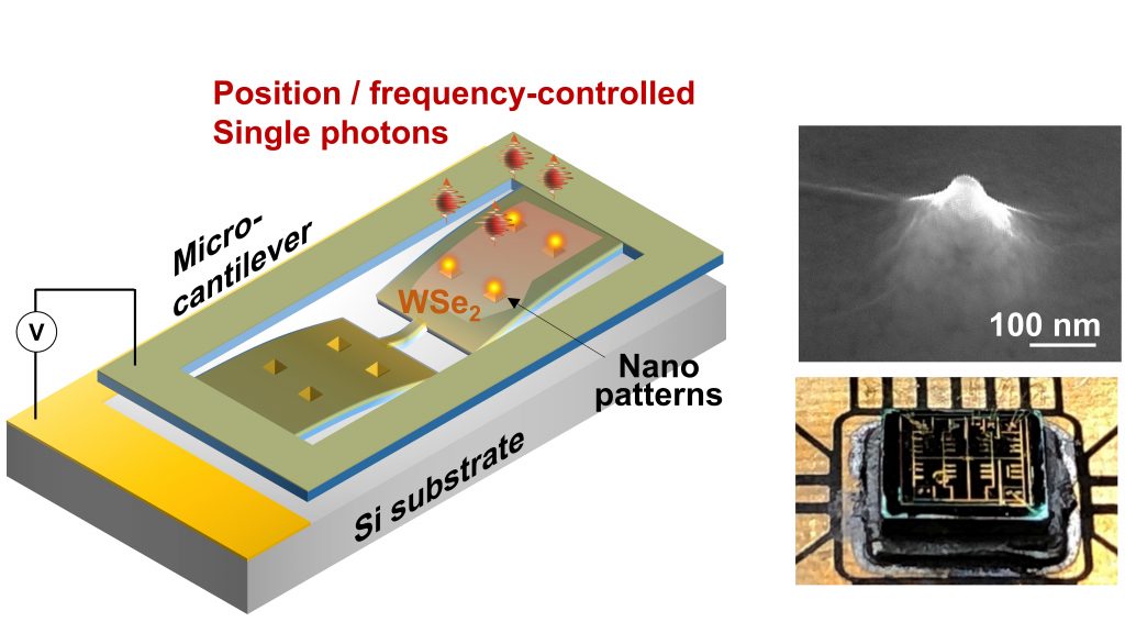
Figure 1. Schematic image of the integrated WSe2 monolayer on the nanopatternd microcantilever after voltage actuation.
In the study, the research team demonstrated simultaneous control of position and frequency of the quantum emitters from transition metal dichalcogenide monolayers. Atomically thin two-dimensional materials are inherently sensitive to external strain and offer a new opportunity of creating and controlling the quantum emitters by engineering strain.
They fabricated an electrostatically actuated microcantilever with nanopyramid patterns, providing a local strain engineering platform for the WSe2 monolayer.
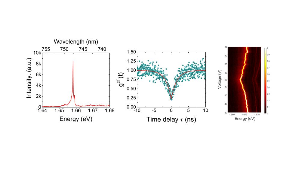
The integrated WSe2 generates high-purity single photon emission at patterned positions with a tuning range up to 3.5 meV. Together with the position and frequency control, they investigated the strain response on the fine-structure splitting and confirm 11% reduction in the fine splitting at the estimated tensile strain of 0.07%.

Figure 2. Photoluminescence spectra of the WSe2 monolayers on patterned regions and the continuous-wave second-order correlation histogram for the quantum emitter shown on left.
“Although various approaches for spatial and spectral control of the quantum emitters have been developed, on-chip control of both position and frequency is still a long-standing goal in solid-state quantum emitters,” says Professor Kim. “Our findings will help provide the basis for unsdestanding the quantum light source-based quantum optics research.”
The findings of this research have been published in the online version of September 2019 issue of Nano Letters. This work has been supported by the National Research Foundation of Korea and Institute of Information and Communications Technology Planning and Evaluation (IITP), funded by the Ministry of Science and ICT (MSIT).
Journal Reference
Hyoju Kim et al., “Position and Frequency Control of Strain-Induced Quantum Emitters in WSe2 Monolayers,” Nano Letters, (2019).


