A research team, led by Professor Jimin Kwon from the Department of Electrical Engineering at UNIST, in collaboration with Professor Yong-Young Noh and his research team from the Department of Chemical Engineering at POSTECH, has announced the successful development of a groundbreaking technology to eliminate defects in molybdenum disulfide (MoS2), a promising candidate for the next generation of semiconductor materials, at a temperature of 200°C.
Modern semiconductor chips, roughly the size of a fingernail, can contain billions of components. MoS2 is emerging as a promising semiconductor material due to its potential for increasing chip density and minimizing leakage current, which ultimately could lead to heat-free, low-power semiconductor chips—drawing significant attention from industry.
Removing defects that occur during the integration of MoS2 into actual chips at low temperatures is a critical challenge for commercialization. This is particularly important because the deposition of MoS2 on silicon devices must be done without damaging existing silicon components, which could be adversely affected by high temperatures.
The research team utilized pentafluorobenzenethiol (PFBT) at 200°C to repair defects in MoS2, achieving a recovery of the atomic ratio of molybdenum to sulfur (Mo:S) to a near-ideal 1:1.98. Typically, during the deposition process, sulfur vacancies (SVs) create defects that lead to an actual ratio of approximately 1:1.68, which hinders electron flow and affects the performance and durability of the semiconductor. Therefore, repairing these defects is essential for restoring the material to its theoretical atomic ratio.
Dr. Haksoon Jung, the lead author, emphasized, “The major advantage of our technique is its compatibility with existing silicon semiconductor back-end-of-line (BEOL) processes, as it can occur at temperatures below 200°C.” He further added, “The BEOL process connects previously deposited components on a substrate and must be conducted below 350°C to prevent damage to the devices.”
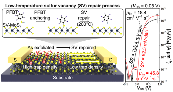 Figure 1. Schematic representation illustrating the low-temperature sulfur vacancy (SV) repair process.
Pentafluorobenzenethiol (PFBT) features a hexagonal benzene ring combined with both a thiol functional group (-SH) and fluorine (-F). The sulfur in the thiol group directly fills the vacancies, while the fluorine facilitates the removal of the non-sulfur portion of the molecule after inducing SVs. The feasibility of this chemical reaction has been confirmed through molecular dynamics simulations. Additionally, X-ray spectroscopy analysis demonstrated that SVs were indeed filled at low temperatures.
Transistor devices made with the repaired MoS2 showed a 2.5-fold improvement in charge mobility compared to devices with defects. Faster charge movement correlates with quicker operational speeds. Moreover, the subthreshold swing value—a critical metric for power consumption—was reduced by approximately 40%.
Professor Kwon stated, “Sulfur vacancy defects that arise during processing represent a significant challenge for semiconductor devices targeting nanoscale advanced nodes.” He further noted, “Through the developed low-temperature sulfur vacancy defect repair technology using organic molecules, we plan to expand our research on defect recovery and interface property improvement in various next-generation semiconductor materials, not only MoS2.”
This research was co-authored by Dr. Haksoon Jung from UNIST and Mingyu Kim from POSTECH and was supported by the Ministry of Science and ICT (MSIT), the National Research Foundation of Korea (NRF), the Institute for Information & communication Technology Planning & evaluation (IITP), and UNIST.
The findings of this study were published in ACS Nano, a prestigious international journal in the field of nanoscience and technology on February 18, 2025.
Journal Reference
Haksoon Jung, Mingyu Kim, Yongwoo Lee, et al., “Back-End-of-Line-Compatible Passivation of Sulfur Vacancies in MoS2 Transistors Using Electron-Withdrawing Benzenethiol,” ACS Nano, (2025).


